科研绘图sci画图作图学术杂志封面设计toc示意图文章配图医学动画


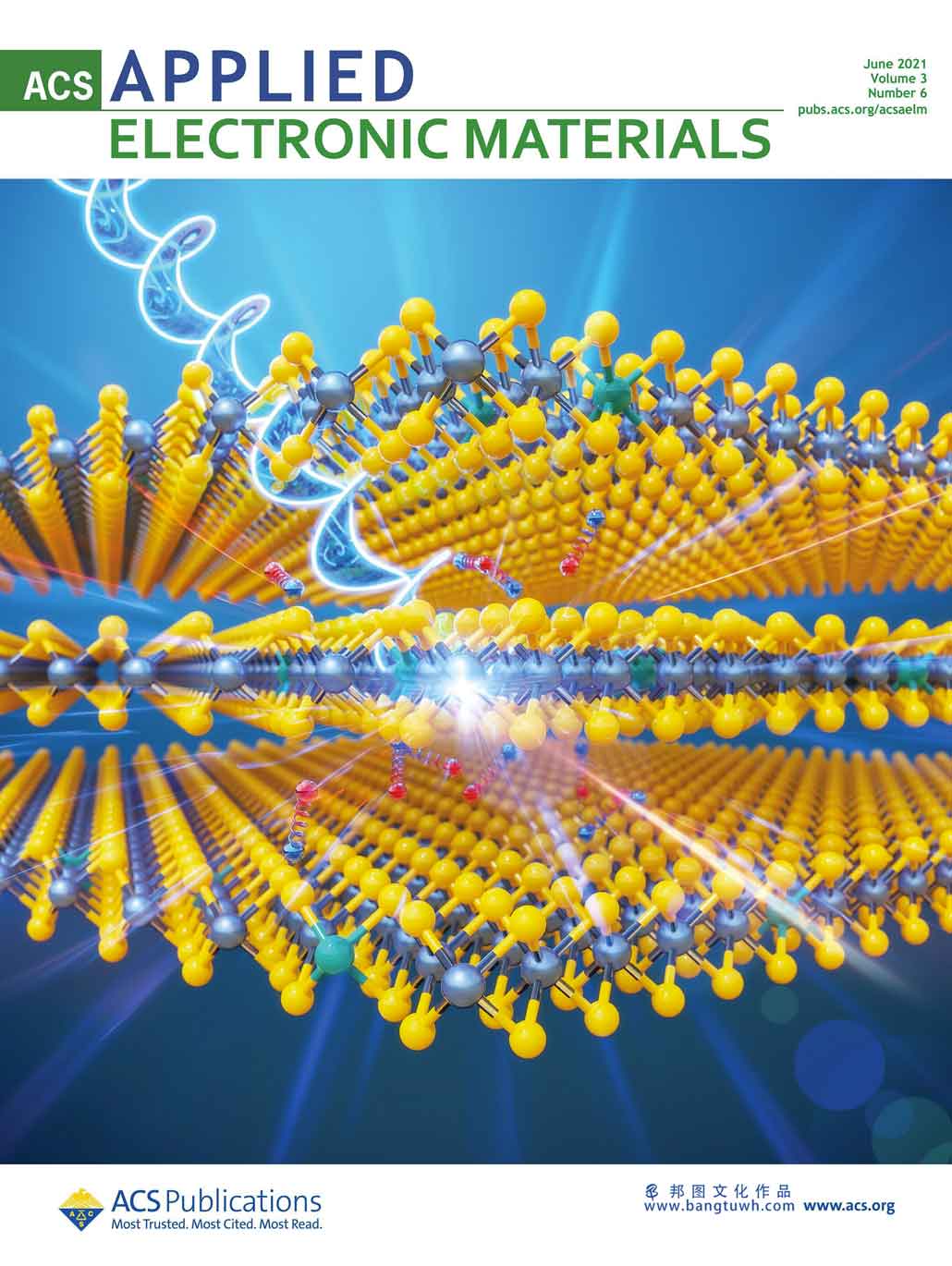
two-dimensional (2d) mos2 has been intensively investigated for its use in the fields of microelectronics, nanoelectronics, and optoelectronics. however, intrinsic 2d mos2 is usually used as the n-type semiconductor due to the unintentional sulfur vacancies and surface gas adsorption. the synthesis and characterization of the 2d mos2 semiconductor of p-type is crucial for the development of relevant p–n junction devices, as well as the practical applications of 2d mos2 in the next-generation cmos integrated circuit. here, we synthesize high-quality, wafer-scale, 2d p-type mos2 (mo1–xnbxs2) with various niobium (nb) mole fractions from 0 to 7.6% by a creative two-step method. the dielectric functions of 2d mo1–xnbxs2 are accurately determined by spectroscopic ellipsometry. we find that the increasing fraction of nb dopant in 2d mos2 can modulate and promote the combination of a and b exciton peaks of 2d mos2. the direct causes of this impurity-tunable combination are interpreted as the joint influence of decreasing peak a and broadening peak b. we explain the broadening peak b as the multiple transitions from the impurity-induced valence bands to the conductive band minimum at k point of brillouin zone by comparing and analyzing the simulated electronic structure of intrinsic and 2d nb-doped mos2. a p-type fet based on the 2d nb-doped mos2 was fabricated for characterization, and its working performance is expected to be adjustable as a function of concentration of nb dopant according to our theoretical research. our study is informative for comprehending optical and electronic properties of extrinsic 2d transitional metal dichalcogenides, which is important and imperative for the development and optimization of corresponding photonics and optoelectronics devices.


微信扫一扫,加设计师好友
17621261539
周一至周五8:30-18:00

提升“研值”

工作人员将在1个小时内联系您。


